Condensed Matter Experiment

The largest research area in physics today deals with the diverse and fascinating properties of condensed matter, encompassing metals, semiconductors, superconductors, polymers, fluids and superfluids, magnets and insulators. This area corresponds to the single largest research group in the department, involving 12 experimentalists and eight theorists.

1


• Scanning tunneling microscopy studies of quantum electronic phenomena and atomic scale reactions at surfaces of semiconductors and low-dimensional materials.

Experimental groups ordinarily consist of a professor, possibly a postdoctoral researcher and several graduate students, with support from a federal source, such as the National Science Foundation or Department of Energy, or from an industrial source.


Group members benefit from each other through sharing of laboratory equipment and expertise, as well as through formal collaborations and materials-related research centers, including the Center for Emergent Materials and the Center for Exploration of Novel Complex Materials. There are also a number of excellent shared research facilities located in the Physics Research Building (see Facilities, Support and Student Groups page).
Yang Group
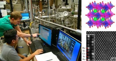
Graduate students Jack Brangham and Jose Flores working on growth of epitaxial films using an MBE-sputtering cluster deposition system in Yang Lab. Top-right: crystal lattice of A2BB'O6 double perovskite oxide. Bottom-right: Scanning transmission electron microscopy image of atomic ordering in a Sr2CrRFeO6 epitaxial film.
 

In addition to strong interactions among the condensed matter experimentalists, a large and active theory group offers expertise in a broad range of subjects. There are about 50 PhD students in condensed matter physics, and at least that many ongoing research projects. They reflect the major directions of current condensed matter research. Some of the problems being investigated are listed below:

  • Magnetic and electronic properties of nanoscale magnetic, semiconducting and metallic systems.
  • Novel approaches to very high resolution scanned probe microscopy.
  • Ultra-high vacuum growth and characterization of complex oxides and other materials with novel magnetic, electronic and thermal properties.
  • Magnetic resonance and ferromagnetic resonance force microscopy of novel materials, device structures and nanostructures.
  • Johnston-Halperin
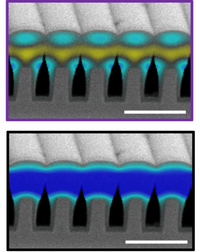
    Electron microscopy image of nanowires formed from a molecule based ultra-low loss ferrimagnet. The color represents the amplitude of quantized magnon (spin-wave) modes in the nanostructures. Scale bar is 500 nm.-Johnston-Halperin Group
  • Optoelectronic, microelectronic and nanoelectronic interface atomic structure.
  • Device physics of polymer-based magneto-optical-electronic device structures.
  • Semiconductor interface growth, processing and characterization by ultra-high vacuum surface science techniques.
  • Schottky barriers and heterojunction band offsets.
  • Raman scattering and magneto-optical imaging of submicron and nanostructures.
  • Brillouin scattering studies of magnetic and elastic properties of hybrid structures and membranes.
  • Manipulation and control of living cells using magnetic fields and nanostructures.
  • Emergent low energy degrees of freedom of complex correlated material systems (quantum matter) using optical spectroscopies with femtosecond and picosecond time resolution.
  • Ultrashort pulses of terahertz and infrared radiation to control/modify quantum matter states.
  • Spin transport in graphene and other two-dimensional materials.
  • Molecular Beam epitaxy of novel magnetic heterostructures.
  • Ultrafast optical microscopy and spectroscopy.
 

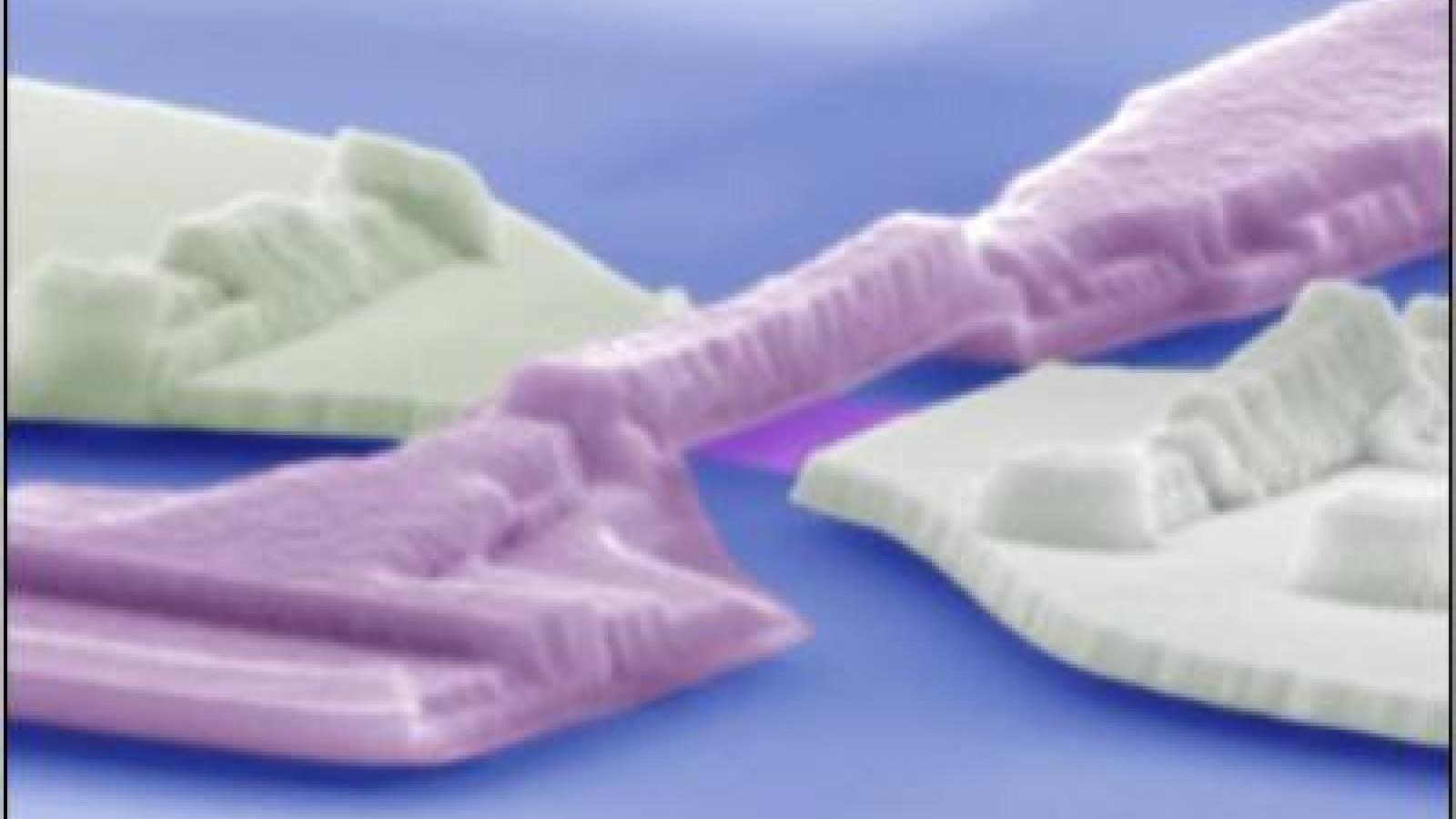
​ * Header Photo: Scanning electron microscope image of a suspended graphene device with suspended top gate. -Lau Group ​


Faculty

PhD, University of California-Berkeley, 1999
Electronics and mechanics of systems that have critical dimensions on the nanometer scale
Transport phenomena that arise in nanostructured materials and learning how to control and detect their mechanical motion

Quantum information

PhD, University of Pennsylvania, 1972
Semiconductor interface growth, processing, and characterization by ultrahigh vacuum surface science techniques
Schottky barriers and heterojunction band offsets
Optoelectronic, microelectronic and nanoelectronic interface atomic structure
Solar cells, bioelectric sensors, ultraviolet microlasers
Ferroelectric/ferromagnetic complex oxides for spintronics and electromagnetic metamaterials
PhD, University of California, Santa Barbara, 2002
Nanoscale studies of organic magnets and conductors
Evolution of electronic and optical properties in nanoclusters
Microscopic studies of spin-scattering in semiconductors
Atomic-scale chemistry on surfaces
PhD, Cornell University, 1984
Magnetic resonance force microscopy
Spin electronics and solid state quantum computing
Nanoscale and multicomponent magnetic systems
Magnetic properties of endohedral fullerenes
PhD, University of California at Santa Barbara, 2003
Spin in reduced dimension
Study of spin dynamics, scattering and transport in nanoscale semiconducting materials
Multifunctional magnetic materials
Development and characterization of magnetic materials with multifunctional properties (magnetization coupled to charge, strain, chemical activity, etc.) for spintronic applications
Spin injection/detection in heterostructures
Exploration of spin injection and detection in heterogenous materials such as metal/semiconductor, organic/inorganic, and molecular/bulk heterostructures
PhD, University of California, Berkeley, 1999
Spin transport in graphene and other two-dimensional materials
Molecular Beam epitaxy of novel magnetic heterostructures
Ultrafast optical microscopy and spectroscopy
PhD, Harvard, 2001   
graphene and two-dimensional materials
quantum transport of charge, spin and heat in nanoscale systems
superconductivity (induced or intrinsic) in nanoscale systems
topological phase and phase transitions
correlated electronic phases and phase transitions
quantum computing
PhD, University of California, Berkeley, 1988
Surface and interface science, scanning tunneling, ballistic-electron emission and atomic force microscopies
Numerical modeling
Nm-resolution electronic behavior of nanostructures, wide bandgap materials, metal/dielectric interfaces and semiconductor surfaces
Surface science, scanning tunneling microscopy
Step dynamics on semiconductor surfaces
Nanoscale properties of buried wide bandgap semiconductor films and interfaces
Nanoscale properties of magnetic multilayers
Atomic scale surface reactions
PhD, University of Illinois 1980
Application and development of spectroscopy probes (Raman scattering, Brillouin scattering and Kerr microscopy) for probing electronic, vibrational, optical and magnetic behavior of novel materials
Magnetic and spin wave excitations and influence of current injection in hybrid micrometer and sub-micron patterned structures
Elastic excitations and guided acoustic resonances in confined geometries
Development of non-invasive techniques for elastic properties of biological tissues
Photo-induced properties of network glasses
PhD, and Director of ENCOMM, Johns Hopkins University, 2001
Fabrication and experimental investigation of structural, electronic and magnetic properties of nanostructured materials
Metallic and oxide epitaxial films
Spintronics in semiconductor nanowires, including spin injection, spin diffusion and spin detection